Fab KiCad Footprint Library
Updated and cleaned up 10/15/2020 by zfredin to fix errors and reflect the homelab inventory; prior footprints to /archive.
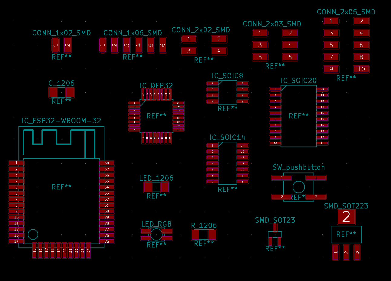
naming convention
fab_x_y_z.kicad_mod
x is category: C, CONN, IC, LED, R, SMD (for generic footprints), etc
y is size/config: 1x06 (single-row 6-pin header connector), SOIC8 (small outline integrated circuit, 8-pin), etc
z is an optional descriptor, such as "SMD" for connectors to differentiate from thru-hole versions
general design strategy
- hand-solderable (i.e., pads should be a bit longer than those intended for automated assembly and reflow soldering)
- route-able using a 1/64" (~0.4 mm) end mill
- maximize bridge span (i.e., space to run two tracks under a 1206 component)
- centered at 0,0
- component outline, reference, and value on F.Silk layer